litopc, in pictures.
A chip is printed with light. Here is how, one picture at a time.
A stencil and a lamp
A chip is printed with light. A stencil on top, a lamp above it, and the wafer below.
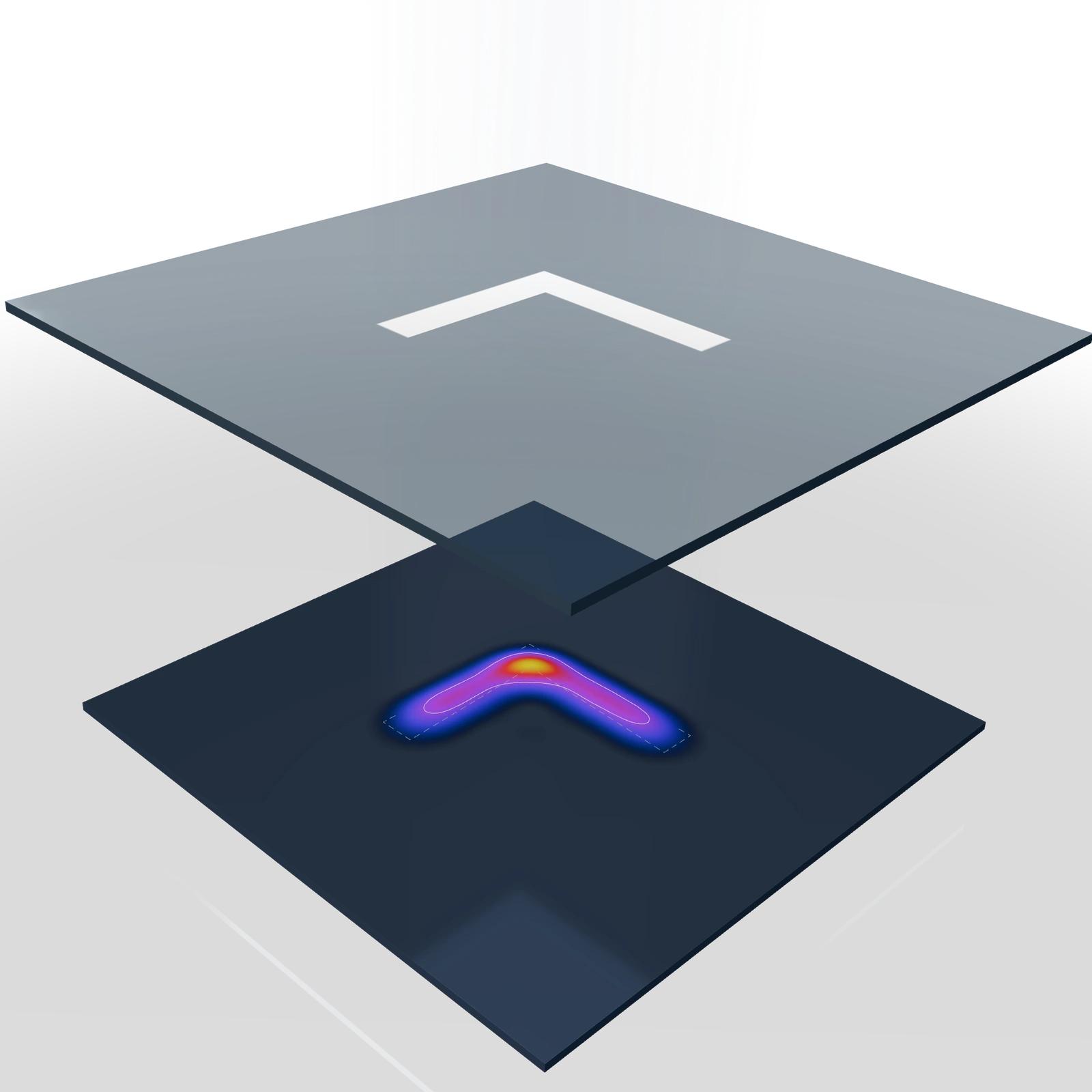 Mask: the stencilLight passes through the LWafer: what gets built
What you draw vs what prints
The shapes are so small that the light blurs on the way down. The print is not the stencil.
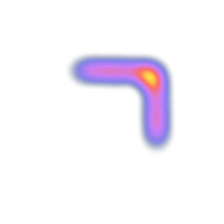
Left: the L you drew. Middle: the light that actually arrives. Right: the shape that prints (solid line) against what you wanted (dashed).
Where the print misses
Corners round off. Line ends pull back. The middle gets thin.
The fix
Where the print came out too small, make the stencil bigger. Where it came out too big, make it smaller. Then check again.
This is optical proximity correction, or opc. The little ears and notches are the nudges. The target never moved; only the stencil did, and now the print lands on it. 5 rounds took the average miss from 25.3 nm to 3.9 nm.
All four steps, in half a minute
The same run, played through. Click a step to jump; switch to 3D at the end.
The target is the shape we want on the wafer; the mask starts as a copy of it.
This L-shape is the design intent. OPC will reshape the mask, never the target.
Recorded from a real litopc run · DUV 193 nm · NA 0.93 · L-corner · threshold 0.3 · 1100 nm field, 512 grid · 80 nm segments · gain 0.5 · 7 samples per edge
In 3D
The same correction in the 3D view: the stencil above, the light on the wafer below.
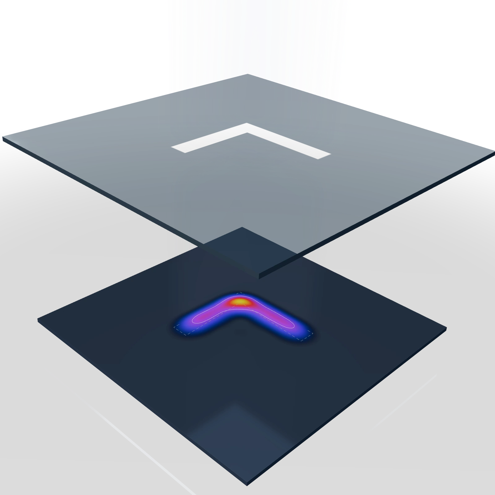 Before correction
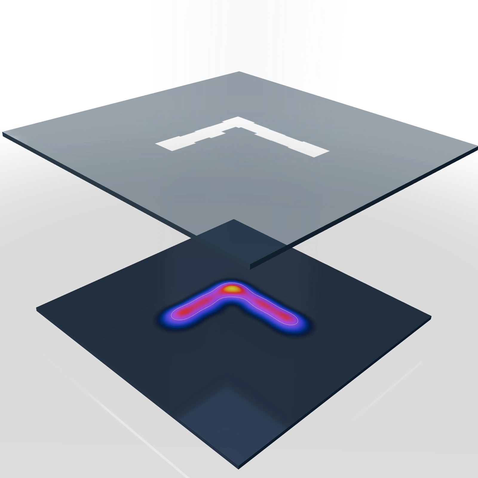 After correction
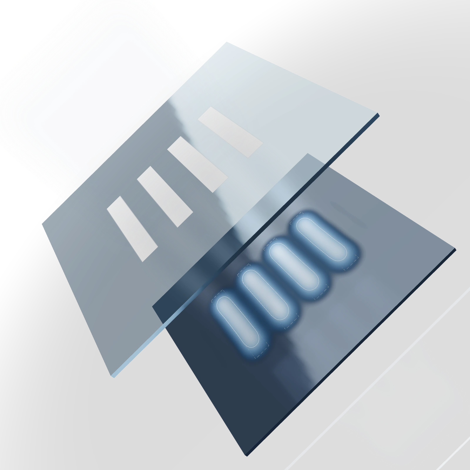
Lines close together
Neighbors matter. Lines drawn side by side print thinner, and their ends fall short.
The brightness knob
The wafer coating only reacts where the light is bright enough. Move the cutoff and watch the printed width change.
- 60 nm linedoes not print
- 90 nm line94 nm
- 140 nm line145 nm
Draw your own
The built-in patterns are a start. Draw any mask from rectangles, set the target, and run the same simulation and correction on it.
This one is two bars and a cut, drawn for the EUV tool: the cut splits the bars into two line ends facing each other across a gap. Simulated and corrected with the same code the simulator runs: the average miss went from 5.4 nm to 1.0 nm in 5 rounds. Free accounts draw up to 5 rectangles and run 3 rounds per correction; Pro, up to 48 rectangles and 5 rounds, then more. Your numbers can differ a little from the recording as the engine evolves.
Glossary
The words used on this site, in the order you meet them.
| Term | Plain meaning | Where you see it |
|---|---|---|
| The setup | ||
| Lithography | Printing a chip's pattern onto silicon with light. | Everything on this site. |
| Wafer, chip | The round silicon plate chips are made on; a chip is one small square of it. | The dark square in the 3D view. |
| Mask, reticle | The stencil that carries the pattern. A DUV mask is a glass plate with chrome on it; an EUV reticle is a mirror with an absorber pattern on top. | The pale plate in the 3D view: lit from above for DUV, from below at an angle for EUV. |
| Target | The shape you want to end up with. | The dashed outline. |
| Field | The square of wafer the simulation covers. | 1100 nm for DUV, 212 nm for EUV; shown as FOV in the simulator. |
| Nanometer (nm) | A billionth of a meter. A hair is about 80,000 nm wide. | Every size here. |
| The light | ||
| Wavelength | The size of one ripple of the light; smaller draws finer detail. | 193 nm (DUV) or 13.5 nm (EUV). |
| DUV | Deep ultraviolet, 193 nm from an ArF laser; the light most chip factories use. It passes through glass, so the tool is a column of lenses. | One of the two tools. |
| EUV | Extreme ultraviolet, 13.5 nm from a tin plasma. Nothing transmits it, so the tool is all mirrors and works in vacuum. | The other tool. |
| NA | Numerical aperture: how wide a cone of light the lens collects; bigger sees finer detail. | 0.93 for DUV, 0.33 for EUV. |
| Partial coherence (σ) | How large the light source looks from the lens. A wider source softens contrast but prints dense lines better. | σ 0.7 in every preset; Pro can shape the source. |
| k1 | Feature size × NA ÷ wavelength: how hard a pattern is for its tool. Near 0.35 the print needs correction to come out right. | The built-in patterns sit around k1 0.35. |
| Aerial image | The light pattern that lands on the wafer after the lens blurs it. | The glowing heat map. |
| Proximity effect | Neighbours change how a shape prints: light from nearby openings spills onto its edges. | Why dense and isolated lines print at different widths. |
| Exposure and focus | ||
| Resist | The light-sensitive coating on the wafer. | Simplified to one brightness cutoff. |
| Threshold (τ) | The brightness that counts as exposed; it stands in for exposure dose. | The slider from 0 to 1; 0.30 prints the default patterns to size. |
| Dose to size | The threshold at which the print comes out exactly as wide as the design. | The 'Size to target' link under the threshold. |
| Defocus | How far the wafer sits from best focus; the image blurs the same way in either direction. | The Defocus slider, in nanometers. |
| Depth of focus | How far focus can drift before the print leaves spec. | The Focus latitude study; the Rayleigh scale is ±112 nm for DUV, ±62 nm for EUV. |
| Bossung curve | Printed width plotted through focus: flat near best focus, falling away on both sides. | The Focus latitude chart. |
| Process window | The range of dose and focus over which the print stays in spec, both at once. | The Process window study (Pro). |
| Measuring the print | ||
| Printed contour | The outline that would really appear on the wafer. | The solid outline. |
| CD | Critical dimension: the width of the printed feature, measured across the centre of the field. | One number per simulation. |
| EPE | Edge placement error: how far the print sits from the target, in nanometers, averaged along the outline. | The number after correction. |
| NILS | How steeply the light falls off at the printed edge, scaled by the feature size; steeper survives dose noise better. | Shown next to CD after each simulation. |
| Corner rounding, line-end shortening | What the blur does to a sharp shape: corners print round and the ends of lines pull back. | Any L-shape or tip-to-tip pattern before correction. |
| Pitch | Centre-to-centre distance of repeated lines or holes. | The dense-lines template; the Through pitch study. |
| Iso-dense bias | The width difference between an isolated feature and the same feature inside a dense group. | The Through pitch reading. |
| MEEF | Mask error enhancement factor: how much a 1 nm change on the mask changes the print. Above 1, mask errors are amplified. | The MEEF study: the slope of wafer CD against mask CD. |
| Correcting the mask | ||
| OPC (optical proximity correction) | Reshaping the stencil so the blurred print comes out right. | The Correct button. |
| Mask bias | Moving every edge of the mask in or out by the same amount: the simplest correction. | The Mask bias study. |
| Segment | A piece of a mask edge that the correction moves on its own. | 80 nm long on DUV, 20 nm on EUV by default. |
| Iteration | One round of simulate, measure, nudge. | 3 per Correct on Free, 5 on Pro; 5 in the replay on the home page. |
| Add, Cut | The two drawing tools: Add places a rectangle, Cut removes one from the shape. | Edit ▸ Target in the simulator. |
| Study | Repeating a run while one setting changes, with a one-line reading of the result. | The Studies tab beside Set-up: 5 points on Free, up to 120 on Pro. |
litopc is for learning and exploring. The pictures are real simulation results, but the model is simplified and not calibrated to any factory. The actual equations are in the model guide; longer reads are on the blog.